Category:Photonics
Vai alla navigazione
Vai alla ricerca
English: Photonics
Français : Photonique
branca dell'ottica .jpg) | |||||
| Carica un file multimediale | |||||
| Istanza di | |||||
|---|---|---|---|---|---|
| Sottoclasse di | |||||
| Parte di |
| ||||
| |||||
Sottocategorie
Questa categoria contiene le 14 sottocategorie indicate di seguito, su un totale di 14.
File nella categoria "Photonics"
Questa categoria contiene 75 file, indicati di seguito, su un totale di 75.
-
 100 TPI fine adjustment screw with close up, Oct 2012.jpg 133 × 217; 12 KB
-
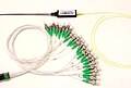 19 channel package plus fibres.jpg 2 884 × 1 940; 674 KB
-
 2010Adlershof.jpg 1 000 × 640; 763 KB
-
 22 nm contact shot noise.png 1 143 × 444; 171 KB
-
 2d pc.png 572 × 474; 10 KB
-
 3D tRR-eps-converted-to.jpg 1 730 × 1 225; 159 KB
-
 AFM-Raman integration.jpg 5 032 × 3 330; 1,27 MB
-
 AFM-Raman microscope.jpg 2 126 × 1 177; 266 KB
-
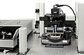
 AFM-Raman-TERS system.jpg 1 024 × 768; 99 KB
-
 Anapoles.png 1 904 × 1 410; 788 KB
-
 Anurag Sharma (Physicist).jpg 1 086 × 1 110; 241 KB
-
 Attocube beamsplitter GWMorley.jpg 5 184 × 3 456; 8,14 MB
-
 Attocube table GWMorley.jpg 5 079 × 3 332; 5,64 MB
-
 CMD dispersion curves.png 900 × 692; 63 KB
-
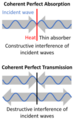 Coherent Perfect Absorption and Coherent Perfect Transmission.png 2 534 × 4 095; 363 KB
-
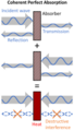 Coherent Perfect Absorption.png 2 826 × 4 950; 457 KB
-
 Continuum Generation in PCF.JPG 2 812 × 1 308; 560 KB
-
 Dual comb chip.png 1 800 × 800; 1,16 MB
-
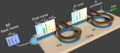
 Dual comb schematic.png 1 478 × 807; 301 KB
-
 Ernst Abbe Equation.jpg 4 032 × 3 024; 5,49 MB
-
 Ernst Abbe Memorial.jpg 3 024 × 4 032; 5,5 MB
-
 FB diagram stacking.png 1 064 × 628; 196 KB
-
 FMN Lab electro-optical integrated modulator.jpg 3 812 × 2 722; 1,81 MB
-
 FMN Lab single photon detector.jpg 1 600 × 1 200; 1,08 MB
-
 FMN Lab team (2).jpg 6 607 × 4 405; 11,34 MB
-
 FSS vs. Eq. Circuit Plot.jpg 960 × 720; 48 KB
-
 General Photonics PSGA101.jpg 503 × 351; 16 KB
-
 Hamamatsu Photonics company logo.svg 664 × 146; 5 KB
-
 Herbert winful portrait.png 843 × 682; 766 KB
-
 Intensity delta is zero.png 1 200 × 900; 11 KB
-
 Lab Mol Colloidal quantum dots 01.jpg 1 600 × 900; 273 KB
-
 Lab Mol Colloidal quantum dots 02.jpg 607 × 1 080; 169 KB
-
 LabBeamCurved.jpg 720 × 400; 57 KB
-
 Laser 01.jpg 1 600 × 1 200; 643 KB
-
 Laser 02.jpg 2 048 × 1 536; 859 KB
-
 Laser 03.jpg 1 536 × 2 048; 1,25 MB
-
-
 LevitatedDiamond GWMorley.jpg 1 518 × 1 135; 354 KB
-
 Levitating nanodiamond GWMorley.jpg 300 × 399; 18 KB
-
 Light Trapping Diagram.png 1 376 × 1 450; 258 KB
-
 Looking at an optical fibre.jpg 5 184 × 3 456; 4,47 MB
-
 Metalens with different focal length and deflection angles.png 1 364 × 1 026; 1,46 MB
-
 Metalens.png 1 336 × 1 004; 1,45 MB
-
 Multi Mode Interferometer.png 450 × 141; 18 KB
-
 Noise distribution.png 1 187 × 1 059; 140 KB
-
 Noise VS Signal Evolution plot.png 562 × 720; 29 KB
-
 Noise VS Signal Evolution pure amplifiers and attenuators.png 862 × 648; 88 KB
-
 Optical parametric amplification.png 709 × 715; 37 KB
-
 Optical parametric oscillation.png 2 864 × 876; 46 KB
-
 Optical-NOT-gate-int.svg 706 × 371; 59 KB
-
 Optical-NOT-gate.png 655 × 354; 78 KB
-
 Panda fiber1.jpg 3 024 × 4 032; 1,02 MB
-
 Panda fiber2.jpg 3 024 × 4 032; 729 KB
-
 Phc1D.png 577 × 121; 9 KB
-
 Phc1Dprofile.png 572 × 208; 26 KB
-
 Photomicrograph of the SPC Test Array.png 204 × 169; 56 KB
-
 Photon arrow.svg 103 × 38; 4 KB
-
 Photonic jet.png 218 × 472; 106 KB
-
 PolControl.png 1 500 × 664; 52 KB
-
 Random laser architectures.png 2 124 × 1 217; 155 KB
-
 Sam-oam-interaction.png 1 085 × 443; 315 KB
-
 Screenshot JCMsuite.png 1 935 × 1 140; 444 KB
-
 SetUp SpectraScan650.png 696 × 797; 551 KB
-
 Summenfrequenz.svg 512 × 183; 32 KB
-
 Table chamber GWMorley.jpg 5 184 × 3 456; 8,62 MB
-
 Table GWMorley.jpg 5 184 × 3 456; 8,26 MB
-
 Thin film coherent perfect absorber.png 1 016 × 601; 90 KB
-
 Titel Photonikbuch.jpg 400 × 600; 90 KB
-
 Trapped diamond July 2016 GWMorley.jpg 3 456 × 2 304; 1,01 MB
-
 U.S. Department of Energy - Science - 408 003 008 (10314800126).jpg 3 344 × 2 324; 623 KB
-
 Variable Optical Attenuator.jpg 820 × 820; 15 KB
-
 Variable Optical Attenuator.svg 60 × 34; 17 KB
-
 Wide band gap phase change material tuned visible photonics.pdf 1 275 × 1 650, 19 pagine; 6,98 MB
-
 Working at an optical communications system testbed.jpg 5 184 × 3 456; 5,52 MB
-
 Синтез фотонных материалов для Индустрии 4.0.jpg 6 000 × 4 000; 3,89 MB


.jpg)


.jpg)


