Category:Wafer bonding
Vai alla navigazione
Vai alla ricerca
packaging technology on wafer-level for the fabrication of microelectromechanical systems etc., ensuring a mechanically stable and hermetically sealed encapsulation | |||||
| Carica un file multimediale | |||||
| |||||
Sottocategorie
Questa categoria contiene le 2 sottocategorie indicate di seguito, su un totale di 2.
P
- Plasma activated bonding (6 F)
R
- Reactive bonding (6 F)
File nella categoria "Wafer bonding"
Questa categoria contiene 48 file, indicati di seguito, su un totale di 48.
-
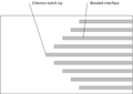 A-chevron1.png 607 × 431; 11 KB
-
 A-chevron1.svg 618 × 458; 6 KB
-
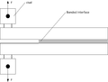 A-chevron2.png 531 × 401; 9 KB
-
 A-chevron2.svg 547 × 440; 8 KB
-
 A-chevron3.png 683 × 567; 23 KB
-
 A-chevron3.svg 755 × 600; 17 KB
-
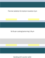
 A-dcb1.png 612 × 251; 11 KB
-
 A-dcb1.svg 652 × 280; 12 KB
-
 A-ir.png 523 × 366; 12 KB
-
 A-ir.svg 582 × 511; 42 KB
-
 A-sheartest1.jpg 655 × 439; 59 KB
-
 A-sheartest2.jpg 655 × 439; 15 KB
-
 A-sheartest3.jpg 655 × 439; 21 KB
-
 B-a-iondriftinglass.png 1 295 × 427; 26 KB
-
 B-a-iondriftinglass.svg 1 268 × 469; 19 KB
-
 B-a-schemeanodicbondprocess.png 978 × 408; 17 KB
-
 B-a-schemeanodicbondprocess.svg 983 × 420; 10 KB
-
 B-ad-bcbprocessflow.png 635 × 850; 27 KB
-
 B-ad-crosssectionbcb.png 3 476 × 2 805; 1,45 MB
-
 B-ad-schematicbondingprocess.svg 476 × 616; 9 KB
-
 B-ad-schematicsu8bondingprocess.png 455 × 595; 11 KB
-
 B-ad-semphotoofsu8.png 2 546 × 1 995; 796 KB
-
 B-d-diagramsurfaceenergy.png 2 477 × 2 114; 324 KB
-
 B-d-hydrophilicsisurface.svg 1 004 × 433; 73 KB
-
 B-e-coatedsurface.png 954 × 190; 9 KB
-
 B-e-coatedsurface.svg 995 × 227; 9 KB
-
 B-e-crosssectionsemofbondinginterface.png 1 694 × 1 153; 1,12 MB
-
 B-e-phasediagram.png 1 811 × 1 471; 83 KB
-
 B-e-ultrasonicimage.png 227 × 230; 56 KB
-
 B-e-ultrasonicimageofblankeutecticwafer.png 373 × 379; 94 KB
-
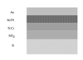
 B-e-wafercomposition.png 341 × 233; 5 KB
-
 B-e-wafercomposition.svg 376 × 271; 8 KB
-
 B-gf-crosssectionsembosch.png 1 511 × 1 182; 262 KB
-
 B-gf-crosssectionsemizm.png 1 501 × 1 164; 285 KB
-
 B-pab-dielectricbarrierdischarge.png 790 × 254; 11 KB
-
 B-pab-dielectricbarrierdischarge.svg 798 × 288; 12 KB
-
 B-pab-plasmareactorlpplasmaactivation.png 689 × 404; 13 KB
-
 B-pab-plasmareactorlpplasmaactivation.svg 723 × 430; 18 KB
-
 B-pab-remoteplasmasystem.png 558 × 264; 12 KB
-
 B-pab-remoteplasmasystem.svg 599 × 303; 15 KB
-
 B-r-bondingprocessmultilayer.png 345 × 247; 10 KB
-
 B-r-bondingprocessmultilayer.svg 730 × 370; 13 KB
-
 B-r-completedreaction.svg 624 × 264; 8 KB
-
 B-r-multilayersystem.png 669 × 462; 459 KB
-
 B-r-schemereactionmultilayer.png 944 × 412; 20 KB
-
 B-r-schemereactionmultilayer.svg 934 × 437; 14 KB
-
 B-tc-tisibondinginterface.png 1 781 × 1 388; 250 KB
-
 Lone Pair P3.png 799 × 562; 18 KB


