File:CMOS NAND Layout.svg
跳转到导航
跳转到搜索

此SVG文件的PNG预览的大小:294 × 587像素。 其他分辨率:120 × 240像素 | 240 × 480像素 | 384 × 768像素 | 513 × 1,024像素 | 1,025 × 2,048像素。
原始文件 (SVG文件,尺寸为294 × 587像素,文件大小:12 KB)
说明
说明
添加一行文字以描述该文件所表现的内容
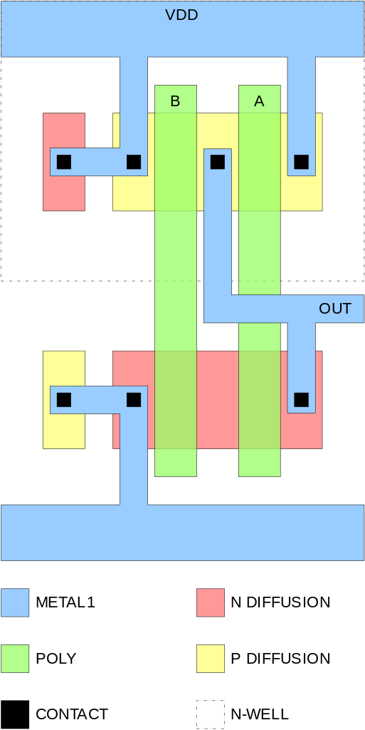
Schematic of CMOS NAND circuit layout
摘要
[编辑]
| 描述 |
English: The physical layout of a CMOS NAND circuit. The larger regions of N-type diffusion and P-type diffusion are part of the transistors. The two smaller regions on the left are taps to prevent latchup.
עברית: שער לוגי מסוג NAND ממבט על.
Polski: budowa bramki NAND CMOS.
Română: Aranjamentul fizic al unei porţi NAND CMOS.
中文:CMOS与非门的布图. CMOS NAND Layout for chip |
| 日期 | 2006年9月7日 (原始上传日期) |
| 来源 | 本檔案是從en.wikipedia轉移到維基共享資源。 |
| 作者 | 英语维基百科的Jamesm76 |
| 其他版本 | 此文件衍生的作品: CMOS AND Silicon.svg |
许可协议
[编辑]
| 本作品已被作者英语维基百科的Jamesm76释出到公有领域。这适用于全世界。 在一些国家这可能不合法;如果是这样的话,那么: Jamesm76无条件地授予任何人以任何目的使用本作品的权利,除非这些条件是法律规定所必需的。 |
原始上传日志
[编辑]
原始描述頁面位於這裡。下列使用者名稱均來自en.wikipedia。
- 2006-09-07 23:46 Jamesm76 294×587×0 (11839 bytes) I am the author and I release this to the public domain.
- 2006-09-07 23:27 Jamesm76 294×587×0 (11827 bytes) SVG drawing of a CMOS NAND gate replacing the older PNG version I had previously uploaded ("CMOS NAND Layout.png"). I am the author and I release this to the public domain.
文件历史
点击某个日期/时间查看对应时刻的文件。
| 日期/时间 | 缩略图 | 大小 | 用户 | 备注 | |
|---|---|---|---|---|---|
| 当前 | 2007年10月19日 (五) 20:46 | | 294 × 587(12 KB) | Prolineserver(留言 | 贡献) | {{Information |Description=''no original description'' |Source=Originally from [http://en.wikipedia.org en.wikipedia]; description page is/was [http://en.wikipedia.org/w/index.php?title=Image%3ACMOS_NAND_Layout.svg here]. |Date=2006-09-07 (first version); |
您不可以覆盖此文件。
文件用途
以下2个页面使用本文件:
全域文件用途
以下其他wiki使用此文件:
- ar.wikipedia.org上的用途
- az.wikipedia.org上的用途
- ca.wikipedia.org上的用途
- en.wikipedia.org上的用途
- en.wikibooks.org上的用途
- en.wikiversity.org上的用途
- es.wikipedia.org上的用途
- fr.wikipedia.org上的用途
- fr.wikiversity.org上的用途
- he.wikipedia.org上的用途
- hi.wikipedia.org上的用途
- ja.wikipedia.org上的用途
- ko.wikipedia.org上的用途
- pl.wikipedia.org上的用途
- ro.wikipedia.org上的用途
- sh.wikipedia.org上的用途
- sr.wikipedia.org上的用途
- zh.wikipedia.org上的用途