Category:Phase-locked loops
Перейти до навігації
Перейти до пошуку
Deutsch: Kategorie:Phasenregelschleifen (PLL).
English: Category:phase-locked loops.
Français : Catégorie:boucles à phase asservie.
Nederlands: Categorie:fasevergrendelingslussen (PLL-schakelingen)..
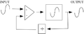
electronic circuit  | |||||
| Завантажити медіафайл | |||||
| Є підкласом | |||||
|---|---|---|---|---|---|
| Складники |
| ||||
| |||||
Файли в категорії «Phase-locked loops»
Показано 200 файлів цієї категорії (із 220).
(попередня сторінка) (наступна сторінка)-
 1 - 1 tolerance with different G.png 1073 × 452; 33 КБ
-
 100 percent frequency uncertainty.pdf 1747 × 1164; 11 КБ
-
 101010 Ph Comp Characteristic.png 1046 × 360; 42 КБ
-
 1st n 2nd contrasted at trans disapp.png 1105 × 475; 28 КБ
-
 1st n 2nd jitter transfer ie noise rejection.png 752 × 508; 51 КБ
-
 1st order loop - pulse response.png 939 × 459; 19 КБ
-
 1st order type 0 slave CDR architecture.png 901 × 389; 25 КБ
-
 1st order type 1 loop.pdf 1754 × 843; 45 КБ
-
 1st order type 1 loop.png 1094 × 754; 56 КБ
-
 2 - 1 tolerance.png 1062 × 455; 32 КБ
-
 2 - 2 and 2 - 1 Application for the De-jitterizer.png 1169 × 604; 153 КБ
-
 2.1 Loop . Filter reference to simulate.png 957 × 304; 16 КБ
-
 2.1 Loop block diagram to simulate.png 1111 × 569; 43 КБ
-
 2.2 Loop . Alternative Filter reference to model n simulate.png 1123 × 731; 52 КБ
-
 2.2 Loop . Filter reference to simulate.png 958 × 303; 16 КБ
-
 2.2 Loop block diagram to simulate.png 1097 × 556; 43 КБ
-
 2013 10 25 1-1 b.b. slew rate for BW.pdf 1754 × 814; 69 КБ
-
 2014 10 12 Slew rate limited 1-1 PLL.png 3237 × 1367; 363 КБ
-

-
 2014 10 27 CDR phase tolerance range vs jitter frequency 2- 2.pdf 1754 × 1239; 505 КБ
-
 2014 10 27 VCO frequency range vs jitter frequency 2- 2.pdf 1754 × 1239; 38 КБ
-
 2014 10 28 CDR phase tolerance range vs jitter frequency 2- 2.png 1788 × 1259; 285 КБ
-

-
 2014 2 26 PDs n PFD free running waveforms.pdf 1579 × 679; 668 КБ
-
 2014 4 27 Waveforms in a 2-2 CDR.png 1380 × 856; 267 КБ
-
 2014 5 15 Sinusoid properties.png 742 × 601; 38 КБ
-
 2015 1 1 onset of triangular SR in 2.2.pdf 1754 × 914; 73 КБ
-
 2015 12 20 6 Single pole filter for 2-1 CDR.pdf 1487 × 1087; 42 КБ
-

-
 2015 2 14 Jitter transfer bandwidths.pdf 1770 × 1010; 45 КБ
-
 2015 3 11 Approx 1 + 2.svg 918 × 241; 190 КБ
-
 2015 3 11 Approx 3 + 4.svg 920 × 233; 191 КБ
-
 2015 3 11 Approx 5 + 6.svg 919 × 224; 192 КБ
-
 2015 3 15 Approx 7 + 8.svg 902 × 189; 186 КБ
-
 2015 3 21 Approx 1 + 2.pdf 1650 × 447; 84 КБ
-
 2015 3 22 Approx 3 + 4.pdf 1650 × 443; 126 КБ
-
 2015 3 22 Approx 5 + 6.pdf 1650 × 420; 115 КБ
-
 2015 3 22 Approx 7 + 8.pdf 1650 × 435; 120 КБ
-
 2015 3 25 Approx 1 + 2.svg 705 × 177; 180 КБ
-
 2015 3 25 Approx 3 + 4.svg 758 × 167; 237 КБ
-
 2015 3 25 Approx 5 + 6.svg 758 × 149; 226 КБ
-
 2015 3 25 Approx 7 + 8.svg 815 × 170; 229 КБ
-
 2015 4 1 Dejitter via phase al.svg 602 × 439; 217 КБ
-
 2016 1 12 tolerance and modulation index 1 - 1 bbang.png 1565 × 1205; 175 КБ
-
 2016 1 12 tolerance and modulation index 2 - 1 linear.png 1565 × 1205; 173 КБ
-
 2016 1 12 tolerance and modulation index 2 - 2 bbang.png 1532 × 1179; 207 КБ
-
 2016 3 5 DeJitterizer with parallel processing.png 673 × 496; 76 КБ
-
 2106 3 7 De-jitterizer (full speed clocks).png 1148 × 524; 126 КБ
-
 2nd order type 1 loop, 3 examples.pdf 1754 × 1239; 59 КБ
-
 2nd order type 2 linear model with jitter transfer equation.png 749 × 431; 27 КБ
-
 2nd order type 2 loop, 3 examples.pdf 1754 × 1239; 59 КБ
-
 3 loops go free running.png 1010 × 360; 31 КБ
-
 Acquisition 1st order.png 1065 × 420; 33 КБ
-
 Acquisition after some slips back and forth total lock delay 2 pi.png 1059 × 411; 61 КБ
-
 Acquisition and tracking of the bang bang 1 -1 loop.png 994 × 504; 72 КБ
-
 Acquisition of a 2-2 with bang-bang PFD.pdf 1754 × 1239; 116 КБ
-
 Acquisition of the bang bang 1 -1 loop density 100%.pdf 1670 × 739; 61 КБ
-
 Acquisition of the bang bang 1 -1 loop density 50%.pdf 1668 × 727; 58 КБ
-
 Acquisition of the bang bang 1 -1 loop Fig 2.png 994 × 511; 68 КБ
-
 Acquisition of the bang bang 1 -1 loop tol lim.pdf 1754 × 814; 70 КБ
-
 Acquisition of the bang bang 1 -1 loop, transition density 100%.png 1385 × 583; 113 КБ
-
 Acquisition of the bang bang 1 -1 loop, transition density 50%.png 1385 × 583; 103 КБ
-
 All Degital PLL (block diagram-2).PNG 1080 × 700; 66 КБ
-
 All Digital PLL (block diagram).PNG 960 × 400; 35 КБ
-
 All Digital PLL (DCO).PNG 440 × 640; 26 КБ
-
 All Digital PLL (MOS Varactor characteristic).PNG 760 × 700; 53 КБ
-
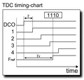 All Digital PLL (TDC timing-chart).PNG 750 × 710; 43 КБ
-
 All Digital PLL (TDC).PNG 1000 × 680; 48 КБ
-
 An example of elastic buffer.svg 394 × 234; 45 КБ
-
 Analog PLL (block diagram).PNG 960 × 400; 32 КБ
-
 Bang bang Phase Detector with “hold”.jpg 1489 × 861; 206 КБ
-
 Bang – Bang Phase Detector.png 929 × 456; 26 КБ
-
 Bang-bang PFD acquisition.png 1390 × 830; 189 КБ
-
 Bang-bang PFD waveforms constant Df random input.png 1385 × 584; 87 КБ
-
 Bang-bang PFD waveforms constantDf 101010 input.png 1385 × 653; 84 КБ
-
 Bang-bang PFD with constant input difference.png 1385 × 624; 93 КБ
-
 Bang-bang Phase and Frequency Detector.png 1489 × 615; 121 КБ
-
 Bang-bang Phase Detector with “hold”.pdf 1754 × 1239; 71 КБ
-
 Block diagram and noise equations 1-1.png 854 × 366; 25 КБ
-
 Block diagram and noise equations 2-1.png 1529 × 657; 186 КБ
-
 Block diagram and noise equations 2-2.png 858 × 364; 27 КБ
-
 Cascade of two CDRs with just different char frequency.png 748 × 320; 18 КБ
-
 CDR based on 2nd PLL simple filter omega zeta vs G tau.png 794 × 350; 23 КБ
-
 CDR basic architecture 2.png 531 × 190; 23 КБ
-
 CDR PSDs and modulations.pdf 1152 × 1641; 97 КБ
-
 CDR std 2nd PLL and variables.png 960 × 720; 15 КБ
-
 CDR std 2nd PLL n variables.png 960 × 720; 14 КБ
-
 CDR2 2 – 1 - actual shortcomings versus the ideal.png 627 × 439; 60 КБ
-
 Char of a lin phase comp for different DT.pdf 1614 × 454; 34 КБ
-
 Char of a linear phase comp for different DT.png 1385 × 391; 113 КБ
-
 Charge pump and filter.png 1034 × 443; 33 КБ
-
 Charge pump.png 591 × 336; 17 КБ
-
 ChargePumpPLLCircuit.svg 125 × 168; 11 КБ
-
 Clock distribution.png 1165 × 260; 22 КБ
-
 Clock paths in the same domain.svg 830 × 380; 112 КБ
-
 De Jitterer characteristics.png 785 × 313; 19 КБ
-
 Definition of Phase Aligner..pdf 1500 × 1125; 91 КБ
-
 Dejittering node.png 753 × 361; 24 КБ
-
 Dejitterizing node Djv std.svg 697 × 348; 99 КБ
-
 Delay locked loop, 0th order type 0 and 1st order type 1.png 935 × 596; 72 КБ
-
 Digital PLL (block diagram).PNG 960 × 400; 38 КБ
-
 Divide 4.png 304 × 160; 5 КБ
-
 Divide 4.svg 512 × 269; 5 КБ
-
 Dual modulus prescaler frequency synthesiser.svg 530 × 280; 23 КБ
-
 Early-late gate PD w hold n table.pdf 1754 × 1239; 61 КБ
-
 Elastic buffer operation.png 1578 × 1145; 219 КБ
-
 Error signal 1 - 1.png 1123 × 794; 2,55 МБ
-
 Error signal 2 - 1.png 942 × 333; 19 КБ
-
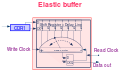
 Example of elastic buffer.png 430 × 273; 12 КБ
-
 Eye sampling in PDs.png 1360 × 830; 73 КБ
-
 Faasilukk.png 592 × 317; 25 КБ
-
 FILTRE1O.jpg 576 × 577; 8 КБ
-
 FILTRE2O.jpg 1194 × 832; 17 КБ
-
 Filtro.png 1108 × 821; 25 КБ
-
 Freq synth.svg 530 × 220; 20 КБ
-
 Gains and characteristics of bang-bang detectors.pdf 1754 × 1068; 64 КБ
-
 Generic PLL diagram with OpAmp filter.png 887 × 600; 31 КБ
-
 Hold in.svg 512 × 294; 1,39 МБ
-
 Hold-in-expl2 4.svg 512 × 296; 9 КБ
-
 Hold-in-expl2 5.svg 512 × 296; 9 КБ
-
 I and Q instants and intervals.pdf 1183 × 316; 16 КБ
-
 I and Q instants and time intervals.png 966 × 195; 28 КБ
-
 ITU-T G823 Fig 13 figure type.pdf 1754 × 1239; 30 КБ
-
 Jitter tol 2-1 with slop. asympt.png 1530 × 903; 158 КБ
-
 Jitter tolerance also 2-1 and 2-2 zeta 0.5 omegan 3.14e6.png 1054 × 454; 33 КБ
-
 Jitter tolerance phase aligners.png 1074 × 488; 36 КБ
-
 Jitter transfer functions 1 1 , 2 1 , 2 2.pdf 1754 × 1239; 60 КБ
-
 Jitter transfer functions 1 1 , 2 1 , 2 2.png 1122 × 794; 88 КБ
-
 Linear PLLs structures definitions.png 646 × 720; 170 КБ
-
 Locked state pll 2.svg 512 × 648; 3,68 МБ
-
 Locked state pll 3.svg 512 × 571; 1,99 МБ
-
 Locked state pll.svg 512 × 599; 3,68 МБ
-
 Loop filter diagram inside a 2nd order PLL.png 723 × 219; 12 КБ
-
 Lowpass jitter filtering.pdf 1239 × 1754; 95 КБ
-
 Model functions 1 - 0.pdf 1754 × 1239; 69 КБ
-
 Model functions 1 - 1.pdf 1754 × 1239; 72 КБ
-
 Models of the characteristic of bang-bang detectors.pdf 1754 × 1068; 33 КБ
-
 Non-linear PLLs structures definitions.png 656 × 719; 182 КБ
-
 Norm error functions 1 1 , 2 1 , 2 2.png 1115 × 569; 53 КБ
-
 Norm tolerance functions 1 1 , 2 1 , 2 2.png 916 × 443; 29 КБ
-
 One wire only.png 789 × 348; 18 КБ
-
 Oscillator spectrum.pdf 1652 × 789; 45 КБ
-
 Pass PFD.png 844 × 400; 26 КБ
-
 Phase and Frequency Detector PFD.jpg 1365 × 640; 197 КБ
-
 Phase Detector using DETFFs and clocks I (lead) and Q (lag) at f 2.pdf 1754 × 1239; 86 КБ
-
 Phase locked loop cs.svg 1064 × 629; 12 КБ
-
 Phase locked loop.svg 1064 × 629; 10 КБ
-
 Phase-locked loop.png 581 × 355; 7 КБ
-
 Phasenrauschen(2).png 646 × 465; 52 КБ
-
 PLL Blockschaltbild.png 493 × 273; 2 КБ
-
 PLL F ARCHITECTURE.jpg 1168 × 310; 21 КБ
-
 PLL F BOUCLE FERMEE.jpg 587 × 720; 20 КБ
-
 PLL F BOUCLE OUVERTE.jpg 582 × 724; 21 КБ
-
 PLL F BRUIT DE PHASE.jpg 585 × 730; 23 КБ
-
 PLL F FILTRE STABLE.jpg 586 × 729; 22 КБ
-
 PLL F STABILITE.jpg 607 × 796; 33 КБ
-
 PLL frequency synthesizer 2.svg 1828 × 1160; 40 КБ
-
 PLL generic inline optional N.png 900 × 200; 17 КБ
-
 PLL generic inline optional N.svg 1026 × 186; 8 КБ
-
 PLL generic inline.svg 900 × 200; 11 КБ
-
 PLL generic it.svg 650 × 245; 11 КБ
-
 PLL generic.svg 633 × 239; 7 КБ
-
 PLL usage it.svg 720 × 190; 10 КБ
-
 PLL usage.svg 521 × 114; 20 КБ
-
 PLL,generic.png 629 × 239; 4 КБ
-
 PLL,usage.png 800 × 242; 14 КБ
-
 PLL-Block.PNG 398 × 90; 3 КБ
-
 PLL-DetectorFase-JK.png 374 × 355; 10 КБ
-
 PLL-detectorFase-XOR.png 392 × 372; 11 КБ
-
 PLL-detectorFrecFase.png 254 × 209; 8 КБ
-
 PLL-phase-model-01.jpg 1642 × 526; 177 КБ
-
 Pll.png 768 × 288; 3 КБ
-
 PLL1 de.svg 400 × 205; 18 КБ
-
 PLL1 it.svg 400 × 205; 16 КБ
-
 PLL1.PNG 398 × 213; 6 КБ
-
 PLL1.png 549 × 254; 10 КБ
-
 PLL2.PNG 447 × 100; 3 КБ
-
 Ring Oscill DJv pdf IS.svg 563 × 506; 29 КБ
-
 Sagedussünt.png 596 × 336; 18 КБ
-
 Schema PLL.png 540 × 282; 8 КБ
-
 Schematic of PLL 1st order.png 571 × 199; 9 КБ
-
 Schematic of PLL 2nd order.png 498 × 368; 18 КБ
-
 Schematic of simulated PLL Rev. 2.png 960 × 720; 50 КБ
-
 Schematic of simulated PLL.png 908 × 613; 34 КБ
-
 Set diagram of CDRs and PLLs.png 493 × 423; 60 КБ
-
 SimplePLL.png 415 × 169; 6 КБ
-
 SimplePLL.svg 434 × 166; 11 КБ
-
 Single Zero Filter.png 1155 × 803; 76 КБ
-
 Static gain of comparators.png 1385 × 671; 132 КБ
-
 StatiPFD.png 1123 × 397; 1,28 МБ
-
 Step response of the single zero filter.pdf 1754 × 1239; 16 КБ
-
 Structures definitions and their fit.pdf 1500 × 1125; 56 КБ
-
 Structures.png 1197 × 721; 237 КБ
-
 The Architecture of the PLL of a CDR is defined by two numbers.pdf 1500 × 1125; 40 КБ
-
 The classic (Hogge) phase comparator.png 977 × 461; 78 КБ
-
 The LOS unlocks the CDR.png 610 × 477; 24 КБ
-
 Tol & Transf of CDRs in a de-jitterizer.png 673 × 257; 32 КБ
-
 Tol & Transf of CDRs in a de-jitterizer.svg 673 × 257; 34 КБ
-
 Tol vectors at 0.2.png 1090 × 1144; 107 КБ
-
 Tol vectors at 0.8.png 1090 × 1144; 99 КБ


.png)

.PNG)
.PNG)
.PNG)
.PNG)
.PNG)
.PNG)

.PNG)


.PNG)


.png)


_phase_comparator.png)


