Category:Wafers
Vai alla navigazione
Vai alla ricerca
sottile fetta di materiale semiconduttore  | |||||
| Carica un file multimediale | |||||
| Sottoclasse di | |||||
|---|---|---|---|---|---|
| Materiale usato | |||||
| |||||
Sottocategorie
Questa categoria contiene le 3 sottocategorie indicate di seguito, su un totale di 3.
File nella categoria "Wafers"
Questa categoria contiene 125 file, indicati di seguito, su un totale di 125.
-
 2008Computex Intel Atom Launch at Grand Hyatt Taipei the Fab.jpg 2 736 × 3 648; 2,7 MB
-
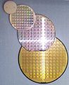
 200mm Si Wafer.png 2 132 × 1 878; 4,74 MB
-
 486 Wafer.jpg 2 000 × 1 986; 2,61 MB
-
 4th Generation Intel® Core™ Processor Wafer Black.jpg 4 288 × 2 848; 10,86 MB
-
 4th Generation Intel® Core™ Processor Wafer White.jpg 4 500 × 3 000; 7,21 MB
-
 6 inch SMIF POD.jpg 3 888 × 2 592; 4,3 MB
-
 A Field of Dreams (40054482212).jpg 3 595 × 3 238; 2,06 MB
-

-
 A Wafer of the Latest D-Wave Quantum Computers (39188583425).jpg 5 158 × 3 522; 3,81 MB
-
 Ausstellung Mikroelektronik in den TSD (09).JPG 1 012 × 978; 710 KB
-
 B-e-ultrasonicimage.png 227 × 230; 56 KB
-

-
 Chips on 6-Inch-Wafer 01.jpg 3 000 × 2 000; 813 KB
-
 CNX Chem 18 00 SilWafer.jpg 1 300 × 381; 1,14 MB
-
 Colorful patterns in the wafers (5900040461).jpg 3 648 × 2 736; 2,22 MB
-
 Computer History Museum (9364488210).jpg 1 600 × 1 067; 563 KB
-
 Drahtsägenprozess wikipedia.JPG 480 × 299; 27 KB
-
 Etchedwafer.jpg 286 × 350; 23 KB
-
 Exposed 150mm 6" wafer with hundreds of chips.jpg 7 118 × 5 122; 8,86 MB
-
 Fale - Monaco - 71.jpg 1 728 × 2 304; 1,15 MB
-
 Fale - Monaco - 72.jpg 2 304 × 1 728; 1,29 MB
-
 Fale - Monaco - 74.jpg 2 304 × 1 728; 1,2 MB
-
 Fale - Monaco - 76.jpg 2 304 × 1 728; 1,15 MB
-
 Fale - Monaco - 80.jpg 2 304 × 1 728; 1,24 MB
-
 Fale - Monaco - 81.jpg 2 304 × 1 728; 1,11 MB
-
 Fale - Monaco - 83.jpg 1 728 × 2 304; 1 023 KB
-
 Front opening shipping box (bottom side).jpg 1 728 × 2 304; 673 KB
-
 Front opening shipping box (front side).jpg 2 304 × 1 728; 767 KB
-
 FUJITSU SPARC64 VIIIfx - 4134068547.jpg 5 616 × 3 744; 5,2 MB
-
 FUJITSU SPARC64 VIIIfx.jpg 5 616 × 3 744; 3,74 MB
-
 Ghost in the Quantum Machine (25215168597).jpg 3 175 × 2 998; 2,35 MB
-
 Haswell Chip.jpg 3 924 × 2 848; 3,33 MB
-

-
 InP Mult-Project Wafer.jpg 1 200 × 769; 511 KB
-
 Intel 8080 open-closed-wafer.jpg 594 × 986; 207 KB
-

-
 Jsc2021e066969.jpg 7 897 × 5 265; 2,73 MB
-
 Klassieren.jpg 1 245 × 1 658; 299 KB
-
 Latest D-Wave 2000 Qubit Processor (25215169297).jpg 1 935 × 1 645; 775 KB
-
 Lighter mit2x - Honeywell 5429-Wafer - John McMaster.jpg 2 626 × 2 542; 1,68 MB
-
 Logo symbol - Honeywell 5429-Wafer - John McMaster.jpg 221 × 235; 9 KB
-
 Logo text - Honeywell 5429-Wafer - John McMaster.jpg 682 × 104; 12 KB
-
 Lyon.Marchande de gaufres.jpg 1 189 × 771; 195 KB
-
 Microelectronics Lab.jpg 506 × 492; 63 KB
-
 Microprocesseurs sur une tranche de silicium.JPG 3 008 × 2 000; 4,11 MB
-
 Monokristalines Silizium für die Waferherstellung.jpg 220 × 588; 34 KB
-
 Mounted wafer.jpg 320 × 270; 42 KB
-
 MPC on Si.png 1 263 × 902; 3,26 MB
-
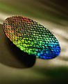
 Multicrystalline silicon wafer with thin film iridescence.jpg 3 286 × 2 041; 1,31 MB
-
 Multicrystallinewafer 0001.jpg 2 359 × 2 335; 1,41 MB
-
 Nanoscope.jpg 4 288 × 2 848; 6,6 MB
-
 Notch and Flat 01.jpg 2 000 × 1 461; 387 KB
-
 Oblea chips.png 189 × 166; 64 KB
-
 Onwafer 510093-b mcmaster mz mit1x.jpg 43 566 × 42 155; 322,68 MB
-
 Onwafer 510131 mcmaster mz mit1x.jpg 43 598 × 42 482; 419,19 MB
-
 Onwafer 610092-a mcmaster mz mit1x.jpg 44 271 × 44 271; 416,02 MB
-
 Overview - Honeywell 5429-Wafer - John McMaster.jpg 1 811 × 1 525; 646 KB
-
 Overview - micrel 6-2807a 8a31099 13 - John McMaster.jpg 2 132 × 1 556; 838 KB
-
 Oxidwafer.jpg 325 × 233; 16 KB
-
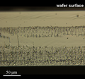
 Panasonic 8 inch wafer surface 1.JPG 2 272 × 1 704; 610 KB
-
 Panasonic chips in tray.JPG 2 272 × 1 548; 637 KB
-
 Photoluminescence image calibrated with PCD on annealed silicon wafer.svg 1 333 × 1 084; 1,81 MB
-
 Photoresist spin coating.jpg 3 452 × 1 594; 1,82 MB
-

-
 Plessey Semiconductors Ltd GaN-on-Silicon microLED arrays on wafer.png 1 059 × 743; 1,91 MB
-
 POWER9TOP500Certificates.jpg 3 111 × 4 148; 8,19 MB
-
 Quantum Annealing - 5714485682.jpg 2 897 × 2 755; 3,54 MB
-
 Quantum Supremacy (39188582795).jpg 1 526 × 1 169; 538 KB
-
 Semiconductor Wafer of Microelectronics.jpg 3 840 × 2 160; 3,06 MB
-
 Shanghai Copper (54220105).jpg 1 501 × 1 645; 1,11 MB
-
 Si wafer 12in.jpg 3 024 × 4 032; 3,18 MB
-
 Si wafer.jpg 4 032 × 3 024; 2,91 MB
-
 Si-rGO.png 2 972 × 1 994; 3,41 MB
-
 Si-Wafer.png 523 × 177; 6 KB
-
 SiC wafers 6inch.jpg 886 × 638; 173 KB
-
 Silicon.JPG 3 872 × 2 592; 4,69 MB
-
 Siliziumwafer-Stapel, der mithilfe einer Diamantdrahtsäge hergestellt wurde.jpg 3 840 × 2 160; 915 KB
-
 Siliziumwafer.JPG 1 264 × 702; 94 KB
-
 Spinner.jpg 641 × 823; 63 KB
-
 Splitted Wafer.png 1 218 × 737; 954 KB
-
 Stealth diced Si wafer 150μm 430x400 MB11.png 430 × 400; 294 KB
-
 Sugar cakes in the recipe books of Margaret Home Countess of Moray.jpg 3 001 × 2 435; 1,32 MB
-
 Tetrahedral amorphous carbon thin film.jpg 1 600 × 1 309; 149 KB
-
 The Beauty of Quantum Computers (25215168907).jpg 2 140 × 2 556; 1,34 MB
-
 The Beauty of Quantum Computers.jpg 1 951 × 2 459; 1,19 MB
-
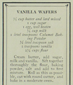 The Childrens Party Book - Vanilla Wafers.png 621 × 717; 641 KB
-
 U.S. Department of Energy - Science - 271 004 006 (9788999284).jpg 3 000 × 1 983; 454 KB
-
 Wafer - 1.jpg 3 264 × 2 448; 714 KB
-
 Wafer - 2.jpg 2 106 × 1 579; 395 KB
-
 Wafer - 3.jpg 1 965 × 1 474; 311 KB
-
 Wafer - 4.jpg 2 592 × 1 944; 419 KB
-
 Wafer - 5.jpg 2 592 × 1 944; 449 KB
-
 Wafer - Legerity 9613 - John McMaster.jpg 1 992 × 1 803; 936 KB
-
 Wafer 1 20140922.jpg 4 928 × 3 264; 5,28 MB
-
 Wafer 1020 - Synertek 1020 - John McMaster.jpg 2 516 × 2 160; 701 KB
-
 Wafer 2 20140922.jpg 4 284 × 2 855; 2,63 MB
-
 Wafer 2 Zoll bis 8 Zoll 2.jpg 557 × 454; 90 KB
-
 Wafer 2 Zoll bis 8 Zoll.jpg 454 × 557; 84 KB
-
 Wafer 20110212.jpg 1 535 × 1 157; 567 KB
-
 Wafer 8K.png 7 296 × 5 472; 29,02 MB
-
 Wafer at Intel Museum.JPG 3 358 × 2 998; 1,52 MB
-
 Wafer die's yield model (10-20-40mm) - Version 2 - DE.png 3 000 × 1 000; 164 KB
-
 Wafer die's yield model (10-20-40mm) - Version 2 - EN.png 3 000 × 1 000; 163 KB
-
 Wafer die's yield model (10-20-40mm).PNG 1 000 × 2 500; 219 KB
-
 Wafer flats convention v2.svg 150 × 150; 13 KB
-
 Wafer flats convention.PNG 190 × 186; 1 KB
-
 Wafer Inspector (5900036077).jpg 2 736 × 3 648; 2,62 MB
-
 Wafer mit 90 Uc61000 chips.jpg 5 381 × 5 344; 15,34 MB
-
 Wafer prober service configuration.jpg 1 500 × 1 165; 684 KB
-
 Wafer through the magnifying glass (5900035793).jpg 3 648 × 2 736; 2,56 MB
-
 Wafer with multiple Microprocessor dies on it.jpg 10 176 × 10 192; 28,12 MB
-
 Wafer with Pentium chips.jpg 1 200 × 1 600; 567 KB
-
 Wafer – Unknown 41-661 – John McMaster.jpg 2 256 × 1 184; 227 KB
-
 Wafer-trasparente.png 557 × 454; 516 KB
-
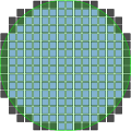 Wafermap showing fully and partially patterned dies.svg 657 × 657; 103 KB
-
 Wafermap.jpg 607 × 615; 70 KB
-
 Wafers (51258425325).jpg 4 912 × 3 264; 8,4 MB
-
 Wafers from 2 to 8 Inches 01.jpg 3 500 × 1 857; 671 KB
-
 Wafers National Museum of Scotland 20.JPG 3 648 × 2 056; 2,65 MB
-
 Wafertraksystem.jpg 2 048 × 1 536; 577 KB
-
 WSI a.JPG 1 600 × 1 200; 611 KB
-
 WSI b.JPG 1 600 × 1 200; 599 KB
-
 WSI Wafer.jpg 849 × 668; 105 KB
-
 Zond A5.jpg 626 × 603; 70 KB
-
 Фотография в кремниевой пластине.jpg 2 592 × 4 608; 5,16 MB


.jpg)
_tape._Few_chips_(dies)_from_the_wafer_have_already_been_picked_up_(removed)_for_further_manufacturing.png)
.jpg)
.JPG)


.jpg)
.jpg)


.jpg)
.jpg)


.jpg)


.jpg)


.jpg)

.jpg)


.jpg)


.jpg)


.jpg)


.jpg)


.jpg)


_-_Version_2_-_DE.png)
_-_Version_2_-_EN.png)
.PNG)