File:Ebers-Moll model schematic (NPN).svg
跳至導覽
跳至搜尋

此 SVG 檔案的 PNG 預覽的大小:250 × 175 像素。 其他解析度:320 × 224 像素 | 640 × 448 像素 | 1,024 × 717 像素 | 1,280 × 896 像素 | 2,560 × 1,792 像素。
原始檔案 (SVG 檔案,表面大小:250 × 175 像素,檔案大小:65 KB)
說明
說明
添加單行說明來描述出檔案所代表的內容
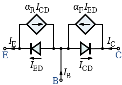
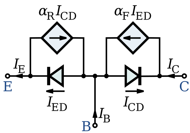
| 描述 | A schematic diagram of the Ebers-Moll models of an NPN BJT. The base, collector and emitter currents are IB, IC and IE, the common-base forward and reverse current gains are αF and αR, and the collector and emitter diode currents are ICD and IED. |
| 日期 | (UTC) |
| 來源 | |
| 作者 |
|
此檔案採用共享創意 姓名標示-相同方式分享 3.0 未在地化版本授權條款。
- 您可以自由:
- 分享 – 複製、發佈和傳播本作品
- 重新修改 – 創作演繹作品
- 惟需遵照下列條件:
- 姓名標示 – 您必須指名出正確的製作者,和提供授權條款的連結,以及表示是否有對內容上做出變更。您可以用任何合理的方式來行動,但不得以任何方式表明授權條款是對您許可或是由您所使用。
- 相同方式分享 – 如果您利用本素材進行再混合、轉換或創作,您必須基於如同原先的相同或兼容的條款,來分布您的貢獻成品。
原始上傳日誌
[編輯].svg&action=edit§ion=1)
This image is a derivative work of the following images:
- File:Ebers-Moll_Model_NPN.PNG licensed with Cc-by-sa-3.0-migrated-with-disclaimers, GFDL-en
- 2010-03-28T19:03:03Z CosineKitty 527x254 (13194 Bytes) Removed incorrect "+" and "-" symbols: charge carriers were backwards for NPN.
- 2010-03-28T18:44:20Z CosineKitty 527x254 (14276 Bytes) Made the following changes to fix errors in the diagram. These changes are based on the diagram on page 903 in ''Microelectronic Circuits, second edition'' by Adel S. Sedra and Kenneth C. Smith, ISBN 0-03-007328-6. 1. Revers
- 2007-09-16T00:43:26Z Kved 527x254 (10811 Bytes) {{Information |Description=NOTE: The diagram has an error. The current through the Base-to-Collector diode should be ICD, not IED. == Summary == Drawn using "Klunky" and added the minor details using MS-WORD |Source=Originall
Uploaded with derivativeFX
檔案歷史
點選日期/時間以檢視該時間的檔案版本。
| 日期/時間 | 縮圖 | 尺寸 | 用戶 | 備註 | |
|---|---|---|---|---|---|
| 目前 | 2011年10月28日 (五) 04:24 | | 250 × 175(65 KB) | Ea91b3dd(對話 | 貢獻) | Corrected the labels on the dependent current sources. They current I subscripts were swapped. |
| 2010年8月4日 (三) 04:48 |  | 250 × 175(31 KB) | Inductiveload(對話 | 貢獻) | {{Information |Description=A schematic diagram of the Ebers-Moll models of an NPN BJT. The base, collector and emitter currents are ''I''<sub>B</sub>, ''I''<sub>C</sub> and ''I''<sub>E</sub>, the common-base forward and reverse current gains are ''α''<su |
無法覆蓋此檔案。
檔案用途
下列頁面有用到此檔案:
全域檔案使用狀況
以下其他 wiki 使用了這個檔案:
- ar.wikipedia.org 的使用狀況
- en.wikipedia.org 的使用狀況
- fr.wikibooks.org 的使用狀況
- he.wikipedia.org 的使用狀況
- uk.wikipedia.org 的使用狀況
- zh.wikipedia.org 的使用狀況
.svg&oldid=461508252)