File:Optoisolator Pinout.svg
跳转到导航
跳转到搜索

此SVG文件的PNG预览的大小:250 × 150像素。 其他分辨率:320 × 192像素 | 640 × 384像素 | 1,024 × 614像素 | 1,280 × 768像素 | 2,560 × 1,536像素。
原始文件 (SVG文件,尺寸为250 × 150像素,文件大小:16 KB)
说明
说明
添加一行文字以描述该文件所表现的内容
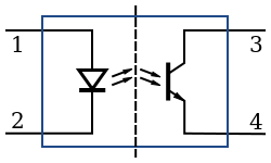
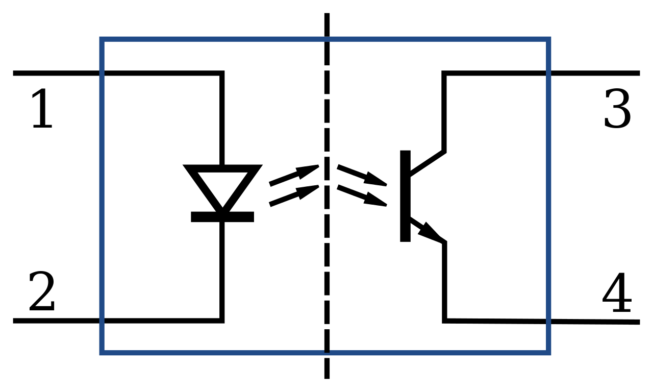
A schematic pinout of an extremely simple opto-isolator device. Often diode and transistor protection and/or amplification will be added. The dashed line in the centre represents to isolation barrer, over which no electrical contact can be permitted.
摘要
[编辑]| 描述 |
English: A schematic pinout of an extremely simple opto-isolator device. Often diode and transistor protection and/or amplification will be added. The dashed line in the centre represents to isolation barrer, over which no electrical contact can be permitted. |
| 日期 | |
| 来源 | 自己的作品 |
| 作者 | Inductiveload |
| 其他版本 |
|


许可协议
[编辑]
| 我,本作品著作权人,释出本作品至公有领域。这适用于全世界。 在一些国家这可能不合法;如果是这样的话,那么: 我无条件地授予任何人以任何目的使用本作品的权利,除非这些条件是法律规定所必需的。 |
文件历史
点击某个日期/时间查看对应时刻的文件。
| 日期/时间 | 缩略图 | 大小 | 用户 | 备注 | |
|---|---|---|---|---|---|
| 当前 | 2008年11月19日 (三) 04:15 | | 250 × 150(16 KB) | Inductiveload(留言 | 贡献) | {{Information |Description={{en|1=A schematic pinout of an extremely simple opto-isolator device. Often diode and transistor protection and/or amplification will be added. The dashed line in the centre represents to isolation barrer, over which no electri |
您不可以覆盖此文件。
文件用途
以下5个页面使用本文件:
全域文件用途
以下其他wiki使用此文件:
- bg.wikipedia.org上的用途
- ca.wikipedia.org上的用途
- de.wikipedia.org上的用途
- en.wikipedia.org上的用途
- es.wikipedia.org上的用途
- et.wikipedia.org上的用途
- eu.wikipedia.org上的用途
- fa.wikipedia.org上的用途
- fi.wikipedia.org上的用途
- fr.wikipedia.org上的用途
- hi.wikipedia.org上的用途
- it.wikipedia.org上的用途
- ja.wikipedia.org上的用途
- pl.wikipedia.org上的用途
- ro.wikipedia.org上的用途
- sv.wikipedia.org上的用途
- uk.wikipedia.org上的用途
- vi.wikipedia.org上的用途
- vi.wikibooks.org上的用途
- zh.wikipedia.org上的用途