File:Wafer flats convention v2.svg

Fitxer original (fitxer SVG, nominalment 150 × 150 píxels, mida del fitxer: 13 Ko)
Llegendes
Llegendes
Resum
[modifica]
| Descripció |
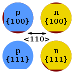
Wafer flats convention, based on Image:Wafer flats convention.PNG Conventional meaning of flats in semiconductor wafers. Red denotes material that has been removed. Wafer orientation is the orientation of the crystallographic plane in which the crystal grew. Wafer type indicated the type of doping.
|
| Data | |
| Font |
self-made, Aquesta imatge vectorial ha estat creada amb Inkscape . |
| Autor | Twisp |
| Altres versions | Wafer flats convention.PNG |
Llicència
[modifica]
| Jo, el titular del copyright d'aquesta obra, l'allibero al domini públic. Això s'aplica a tot el món. En alguns països això pot no ser legalment possible, en tal cas: Jo faig concessió a tothom del dret d'usar aquesta obra per a qualsevol propòsit, sense cap condició llevat d'aquelles requerides per la llei. |
Historial del fitxer
Cliqueu una data/hora per veure el fitxer tal com era aleshores.
| Data/hora | Miniatura | Dimensions | Usuari/a | Comentari | |
|---|---|---|---|---|---|
| actual | 21:40, 24 set 2013 | | 150 × 150 (13 Ko) | Cepheiden (discussió | contribucions) | fixed position of secondary flat Silicon processing for the VLSI era - Vol. 1 - Process technology; S Wolf; RN Tauber - Lattice Press; 1986; ISBN 096167237; p. 23 |
| 00:37, 23 des 2008 |  | 150 × 150 (13 Ko) | Inductiveload (discussió | contribucions) | Added arrow indication <110> direction and enlarged flats so they can be easily seen | |
| 21:17, 29 feb 2008 |  | 150 × 150 (9 Ko) | Twisp (discussió | contribucions) | ||
| 21:13, 29 feb 2008 |  | 150 × 150 (9 Ko) | Twisp (discussió | contribucions) | ||
| 21:06, 29 feb 2008 |  | 150 × 150 (8 Ko) | Twisp (discussió | contribucions) | ||
| 20:59, 29 feb 2008 |  | 150 × 150 (8 Ko) | Twisp (discussió | contribucions) | ||
| 18:09, 29 feb 2008 |  | 150 × 150 (9 Ko) | Twisp (discussió | contribucions) | {{Information |Description= Wafer flats convention, based on Image:Wafer flats convention.PNG Conventional meaning of ''flats'' in semiconductor wafers. Black denotes material that has been removed. Wafer orientation is |
No podeu sobreescriure aquest fitxer.
Ús del fitxer
Les 2 pàgines següents utilitzen aquest fitxer:
Ús global del fitxer
Utilització d'aquest fitxer en altres wikis:
- Utilització a ca.wikipedia.org
- Utilització a cs.wikipedia.org
- Utilització a de.wikipedia.org
- Utilització a en.wikipedia.org
- Utilització a es.wikipedia.org
- Utilització a et.wikipedia.org
- Utilització a eu.wikipedia.org
- Utilització a fi.wikipedia.org
- Utilització a it.wikipedia.org
- Utilització a it.wikibooks.org
- Utilització a ja.wikipedia.org
- Utilització a ko.wikipedia.org
- Utilització a nl.wikipedia.org
- Utilització a pl.wikipedia.org
- Utilització a ro.wikipedia.org
- Utilització a sk.wikipedia.org
- Utilització a uk.wikipedia.org
- Utilització a www.wikidata.org