Category:CMOS
Jump to navigation
Jump to search
technology for constructing integrated circuits | |||||
| Upload media | |||||
| Instance of |
| ||||
|---|---|---|---|---|---|
| Subclass of | |||||
| Discoverer or inventor |
| ||||
| Has use | |||||
| |||||
CMOS = Complementary Metal Oxide Semiconductor Technology
Subcategories
This category has the following 6 subcategories, out of 6 total.
Media in category "CMOS"
The following 83 files are in this category, out of 83 total.
-
 1.SOC.2.B.CMOS.Process.20130320.2.pdf 1,654 × 1,239, 12 pages; 2.21 MB
-
 1.SOC.2.B.CMOS.Process.20130408.2.pdf 1,654 × 1,239, 14 pages; 189 KB
-
 1.SOC.2.B.CMOS.Process.20130430.pdf 1,654 × 1,239, 17 pages; 211 KB
-
 1.SOC.2.C.CMOS.Digital.20130318.2.pdf 1,654 × 1,239, 19 pages; 221 KB
-
 1.SOC.2.D.CMOS.Analog.20130320.pdf 1,654 × 1,239, 10 pages; 384 KB
-
 1.SOC.2.E.CMOS.RC.20130325.pdf 1,654 × 1,239, 17 pages; 501 KB
-
 1.SOC.2.E.CMOS.RC.20130327-2.pdf 1,654 × 1,239, 25 pages; 608 KB
-
 1.SOC.2.E.CMOS.RC.20130327.pdf 1,654 × 1,239, 23 pages; 599 KB
-
 1.SOC.2.E.CMOS.RC.20130430.pdf 1,654 × 1,239, 25 pages; 609 KB
-
 1.SOC.2.F.CMOS.Switching.20130327-2.pdf 1,654 × 1,239, 13 pages; 363 KB
-
 1.SOC.2.F.CMOS.Switching.20130401.pdf 1,654 × 1,239, 19 pages; 348 KB
-
 1.SOC.2.F.CMOS.Switching.20130402.pdf 1,654 × 1,239, 22 pages; 364 KB
-
 1.SOC.2.F.CMOS.Switching.20130403.pdf 1,654 × 1,239, 23 pages; 388 KB
-
 1.SOC.2.F.CMOS.Switching.20131031.pdf 1,654 × 1,239, 24 pages; 394 KB
-
 1.SOC.2.G.CMOS.Sizing.20130403.pdf 1,654 × 1,239, 10 pages; 107 KB
-
 1.SOC.2.G.CMOS.Sizing.20130408.pdf 1,654 × 1,239, 12 pages; 125 KB
-
 1.SOC.2.H.CMOS.Power.20130403.pdf 1,654 × 1,239, 7 pages; 111 KB
-
 1.SOC.2.H.CMOS.Power.20130408.pdf 1,654 × 1,239, 13 pages; 174 KB
-
 3d-cmos-loss-diagram.svg 564 × 449; 805 KB
-
 A CMOS current-mode full-adder cell for multi-valued logic VLSI (IA acmoscurrentmode109457557).pdf 1,275 × 1,650, 119 pages; 20.45 MB
-
 A CMOS VLSI IC for real-time opto-electronic two-dimensional histogram generation (IA acmosvlsiicforre1094539739).pdf 1,275 × 1,650, 94 pages; 3.17 MB
-
 APS-Principle.svg 373 × 143; 12 KB
-
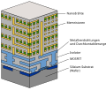
 Aufbau CMOS-Chip 2000er.svg 550 × 810; 84 KB
-
 Bayer Contour XT - board - S35390 Aves 4690-9876.jpg 1,545 × 1,545; 1.54 MB
-
 BSI CMOS.PNG 670 × 609; 23 KB
-
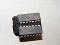
 CD4011 1.png 794 × 1,123; 52 KB
-
 CD4011-2.png 794 × 1,123; 54 KB
-
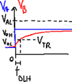
 Characteristic of a H-state CMOS inverter.png 310 × 234; 2 KB
-
 Characteristic of a L-state CMOS inverter.png 239 × 204; 1 KB
-

-

-
 CMOS 4017 - Functional Diagram - Edge Up - with pin number colored.svg 1,064 × 452; 101 KB
-
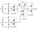
 CMOS Circuit.svg 482 × 415; 25 KB
-
 CMOS cross section FR.png 1,200 × 426; 31 KB
-
 CMOS LNA.jpg 376 × 337; 21 KB
-
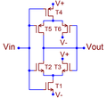 CMOS Schmitt trigger (rearranged to show two long-tailed pairs).png 1,127 × 1,031; 51 KB
-
 CMOS transition times.png 432 × 147; 824 bytes
-
 CMOS TW OSC 000.png 1,283 × 841; 109 KB
-
 CMOS under a microscope 01.jpg 640 × 480; 58 KB
-
 CMOS under a microscope 02.jpg 640 × 480; 56 KB
-
 CMOS under a microscope 03.jpg 640 × 480; 66 KB
-
 Cmos-chip structure in 2000s (en).svg 550 × 810; 138 KB
-
 CMOS-Inverter mit parasitärem Thyristor.png 3,141 × 1,659; 154 KB
-
 CMOS-Logic-ICs 52672-480x360 (4791221977).jpg 480 × 360; 33 KB
-
 CMOS-NOT-NAND.png 1,006 × 1,240; 101 KB
-
 CMOS.ee.png 400 × 385; 27 KB
-
 Cmos.PNG 487 × 202; 6 KB
-
 Cmos2.PNG 400 × 150; 4 KB
-
 Cmosbuff.png 852 × 669; 78 KB
-
 CMOSlüliti.png 572 × 289; 76 KB
-
 Collegamento CMOS a bus con uscite 3S.png 164 × 264; 1 KB
-
 Comparison - sCMOS vs. CCD technology.jpg 992 × 874; 522 KB
-
 Connection CMOSes to bus through OC outputs.png 151 × 237; 900 bytes
-
 CPT-Electronics-CMOS-NPN.svg 70 × 138; 499 bytes
-
 CPT-Electronics-CMOS-PNP.svg 76 × 138; 533 bytes
-
 Electronics Klunky CMOS NPN.PNG 37 × 37; 273 bytes
-
 Electronics Klunky CMOS PNP.PNG 37 × 37; 271 bytes
-
 Fonctionnement d'un circuit en logique CMOS.png 569 × 426; 10 KB
-
 Graphs HL transition CMOS inverter with capacitive load.png 163 × 246; 1 KB
-
 Graphs LH transition CMOS inverter with capacitive load.png 166 × 190; 1,000 bytes
-
 Graphs of CMOS inverter HL transition with capacitive load 2.png 163 × 246; 1 KB
-
 Graphs of CMOS inverter LH transition with capacitive load 2.png 166 × 190; 973 bytes
-
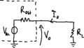 H-state CMOS inverter with resistive load.png 258 × 148; 947 bytes
-
 High Bandwidth Memory schematic (zh-CN).svg 512 × 288; 29 KB
-
 High Bandwidth Memory schematic.svg 960 × 540; 47 KB
-
 Hybrid CMOS Memristor Schaltung 3D.svg 426 × 359; 54 KB
-
 Hybrid CMOS Memristor Schaltung.svg 426 × 359; 23 KB
-
 L-state CMOS inverter with resistive load.png 306 × 148; 1 KB
-
 Latchup ckt.png 404 × 418; 12 KB
-
 Latchup.png 741 × 339; 24 KB
-
 Museum of Moscow Aviation Institute 2016-02-02 012.JPG 2,560 × 1,920; 2.36 MB
-
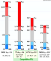 Niveaux logiques CMOS-TTL-LVTTL.png 760 × 900; 56 KB
-
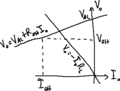
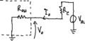
 Pot dinamica media(Vi,Id,t).jpg 962 × 466; 27 KB
-
 Pot dinamica media(Vo,Vi,Id).jpg 875 × 363; 12 KB
-
 Principe de la conception de circuit en technologie CMOS.png 674 × 373; 13 KB
-
 Soviet К190КТ2П CMOS analog switch IC (18591468658).jpg 1,180 × 672; 151 KB
-
 Soviet К190КТ2П CMOS analog switch IC (18991605845).jpg 1,000 × 794; 163 KB
-
 Td7bfig3.png 357 × 150; 13 KB
-
 Transistors CMOS en série.png 613 × 351; 23 KB
-
 Wikitrip to MAI museum 2016-02-02 079.JPG 3,384 × 1,900; 4.74 MB
-
 XC6206 Lower Magnification.jpg 3,401 × 2,809; 1.83 MB
-
 XNOR OAI CMOS.svg 336 × 306; 27 KB
-
 موصل.jpg 12,000 × 9,000; 19.97 MB


.png)


.svg)

.jpg)


.svg)


.jpg)
.jpg)

.jpg)
.jpg)


